Accelerating Innovation with Additive Manufacturing
 The desire to quickly ramp-up production hampers traditional manufacturing workflows in many ways. A capital-equipment manufacturer needing to surge-order a particular part may require more resources than one supplier can handle, and the overhead required to set up an additional supplier may prove prohibitive. And, traditional product development, often lengthy and cumbersome due to the need for tooling, undercuts the desire to create and deliver more productive equipment more quickly.
Additive manufacturing (AM) removes these limitations, enabling freedom of design and a seamless transition from prototyping to low-volume production of bespoke parts. Integrating AM into their traditional manufacturing workflows allows capital-equipment manufacturers to optimize strength-to-weight ratios, add conformal-cooling structures, and reduce system part counts and the need for assemblies. This results in improved fluid dynamics, reduced assembly failures, better kinematics and closer adherence to theoretical operation states. With hundreds of thousands of components required to create a tool, AM offers seemingly limitless options for improving applications. Let’s explore three semiconductor AM options in particular that have demonstrated advantages.
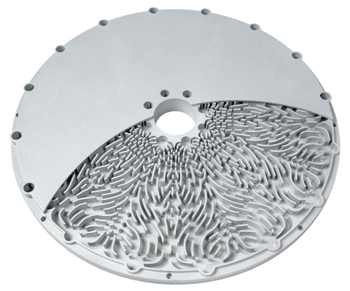
Wafer-Table Thermal Management
 Better thermal management of critical semiconductor-equipment components, such as wafer tables, can improve semiconductor equipment accuracy by 1 to 2 nm and simultaneously improve speed and throughput. Increased machine speed and uptime lead to more wafers processed and a higher overall lifecycle value.
Lithography demands keeping temperatures within milliKelvin (mK) ranges, as any system disturbance has an impact at the nanometer scale. Through design for AM, engineers can optimize internal cooling channels and surface patterns, dramatically improving surface temperatures and thermal gradients while reducing time constants. With unique designs attainable only with AM, components efficiently dissipate heat, enhance system throughput and accuracy, and improve overall performance. For example, a large semiconductor capital-equipment manufacturer using AM to produce its wafer tables realized an 83-percent decrease in ΔT, or change in temperature (13.8 to 2.3 mK), and a five-fold reduction in time to wafer stabilization.
Another benefit of using AM to produce wafer tables: structural optimization and tables with reduced part counts and assemblies. Producing components using traditional technologies relies on brazing to join parts together. Brazing, a lengthy, low-yield process with as much as a 50-percent rejection rate, proves inefficient when a producer desires rapid iteration. Replacing multipart assemblies with monolithic AM parts increases reliability, improves manufacturing yield and reduces labor costs.
Manifold Fluid-Flow Optimization
Using traditional manufacturing processes to produce complex fluid manifolds results in large, heavy parts with non-optimal fluid flow due to abrupt transitions between components, and channels with sharp angles that lead to disturbance, pressure drops, stagnant zones and leakage.
Employing AM to produce these same manifolds allows engineers to optimize designs to reduce pressure drop, mechanical disturbances and vibration. A 90-percent reduction in flow-induced disturbance forces reduces system vibration and realizes a 1 to 2-nm accuracy improvement.
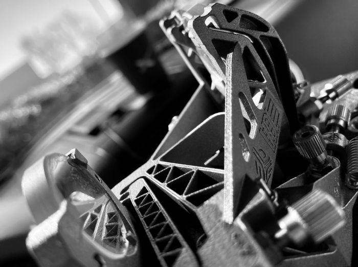
Structural Optimization and Advanced Flexures
AM gives designers the flexibility to optimize the structural topology of a part (i.e., lightweighting) with a suite of high-strength metal alloys. These designs more precisely can meet the performance requirements of semiconductor capital equipment, improve the strength-to-weight ratio and deliver a faster time to market.
Lightweighting of semiconductor components and advanced-motion mechanisms reduces inertia and improves lithography and wafer-processing-machine speed and uptime, leading to more wafers processed. In one example, an equipment manufacturer employed AM to achieve more than a 50-percent weight reduction in flexures and 23-percent-higher resonant frequency, and reduced system vibration.
Limitless Opportunities
AM—specifically direct metal printing—represents a recognized, validated technology in the semiconductor capital-equipment industry. The pressures within the market for optimization, the demand for more equipment and significant production barriers require a rapid movement toward additive. Newly developed wafer-processing equipment includes AM parts, with some of this equipment already being shipped.
Purely from a lithography perspective, a lot of equipment already finds use in production to create chips using a ~14-nm process. AM can affect this existing install base via OEMs creating field upgrades to improve aspects of these systems. However, this is less likely a significantly enabling pathway. More likely: AM will significantly enable newer machines —either shipping today or within the next one to two years. This pathway provides ample time for component- and system-level redesigns that will increase productivity and quality. Additionally, the manufacturers still will retain enough control over these systems to rigorously test and prove performance gains.
Outside of lithography reside dozens of other applications in the process chain, including polishing, light sources and etching, sorting, and even metrology. The expanded use of AM in this segment arrives at a perfect time, as equipment manufacturers speed toward some ‘cliffs of impossibility’ where physics inevitably will create extremely challenging limitations. In this realm, AM more likely will enable and unlock new process levels, though the process won’t eliminate the barriers of physics and the eventuality of some massive shifts in process. However, AM sends such challenges decades into the future, and allows semiconductor-capital-equipment manufacturers to rethink what is possible and push the boundaries. In so doing, AM offers a tremendous opportunity to overcome the semiconductor shortage, and once again strengthen supply chains. 3DMP
See also: 3D Systems
Technologies:


 Scott Green
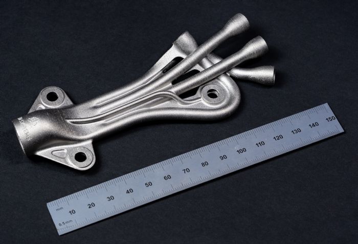 If we need more chips, can’t chip manufacturers just increase manufacturing capacity? This sounds easy enough in theory, but production capacity and technology challenge that intent.